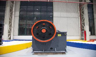
مصنع لتجهيز البوكسيت/mininggrinding mechanical wafer
Abstract: Copper chemical mechanical polishing (CMP) and wafer thinning technologies have been challenges for Through Silicon Via (TSV) interconnect in recent years. In this work, copper CMP slurry and process and wafer level thinning with temporary bonding were studied in detail. The concentration of peroxide (H 2 O 2), citric acid, SiO 2 particle and Benzotriazole (BTA) in the CMP slurry and ...
Grinding of silicon wafers Department of Indust, what is the dimension of 7af grinding machine,dimensional mathematical wafer shape model was established by which three technical issues in wafer grinding were studied, wafer grinding machines, grinding mark elimination, and central bump elimination The wafer shape model in . Get Price
In this study, a novel single step thinning process for extremely thin Si wafers was put forward by use of an integrated cup grinding wheel (ICGW) in which diamond segments and chemo mechanical grinding (CMG) segments are alternately allocated along the wheel periphery. Get Price Continuous variable feed rate A novel method for
Chemical mechanical polishing (CMP) is the primary method to realize the global planarization of silicon wafer. In order to improve this process, a novel method which combined megasonic vibration to assist chemical mechanical polishing (MACMP) is developed in this paper.
Abstract: In order to decrease the development costs, shorten the developing cycle, improve the overall performance and reduce the environmental pollution of the wafer precision grinding machine, the structure, transmission, movement of grinding system for wafer precision grinding machine is analyzed based on mechanical system mechanics, the threedimensional model of the grinding system is ...
Silicon on insulator (SOI) wafers are manufactured by bonding one Si wafer to the other by activating the surface of both wafers and then placing them together so that a strong bond occurs first through the van der Waals attraction and then by forming a covalent bond [59].Activation of the superclean Si surface is the key to accomplish this bonding, typically by a remote plasma process.
The Milliken® product line includes a full line of check valves including: swing check, spring loaded, double disc, globe, compact wafersilent, wafer, flexible .
OKAMOTO Semiconductor Equipment Technology ... Grinding Grinding The machine can grind such semiconductor material as silicon, gallium arsenide, etc. And electronic material as ... Footprint(W xH) mm 2580x 1765x 1784/3610x2227x2119 WorkSi wafer Work size mm rp2001 tP300 Grinder for brittle materials. Get Price; Ancient Grinding Stone Stock Photos
Effect of sawing defects on mechanical strength of PV silicon wafers Kevin Skenes1, Hao Wu1, Frank Mess2, Chris Yang2, Shreyes Melkote1,2 and Steven Danyluk1 1G. W. W. School of Mechanical Engineering, Georgia Institute of Technology, Atlanta, GA, USA 2Manufacturing Research Center, Georgia Institute of Technology, Atlanta, GA, USA Characterize!surface!defects!of!wafers!
What is a Silicon Wafer? Silicon is a gray, brittle, tetravalent, chemical element. It makes up % of the earth's crust and next to oxygen, it is the most abundant element in nature. Some of the most common materials that contain silicon are quartz, agate, flint, and common beach sand, among others.
16 CHAPTER 1 INTRODUCTION General Background The electronics industry has grown rapidly in the past three decades. Ultralargescale integrated (ULSI) circuits, with 108 or more devices on a chip, can now be fabricated on semiconductor substrates, or wafers.
Wafer Thinning. There are four primary ways to thin wafers, (1) mechanical grinding, (2) chemical mechanical planarization, (3) wet etching and (4) atmospheric downstream plasma dry chemical etching (ADP DCE). There are two groups that make up the four wafer .
Precision Grinding of UltraThin Quartz Wafers. · Precision Grinding of UltraThin Quartz Wafers the same apparatus that is used to machine the quartz wafers. Grinding the chuck flat is perhaps the most difficult operation in the proposed wafer grinding process, since porous ceramic actively erodes the .
write the classification of grinding machine BINQ Mining Grinding Machine Gold and marble grinding machine classification. Dec 16, 2011 · 7+ Documents Related to .
Apr 25, 2017 To prepare for mechanical grinding, a wafer is placed on a porous ceramic chuck and held in place by a vacuum. The wafer is situated with its back side facing up towards the grind wheel, while a grind tape is placed on the front side of the wafer to protect it .
Precision Passive Mechanical Alignment of Wafers Alexander H. Slocum, Alexis C. Weber Precision Engineering Research Group, Massachusetts Institute of Technology, 77 Massachusetts Ave, Room 3 445, Cambridge, MA 02139, slocum Abstract A passive mechanical wafer alignment technique, capable of micron and better alignment accuracy,
Okamoto is a leading manufacturer of precision grinding and polishing tools since 1935. Grinding tools used in applications of wafer manufacturing, SOI, TSV, MEMS, thin wafers down to 25 um, bonded wafers, bumped wafers, solar ingot grinding, quartz, sapphire, GaAs, InP and more.